HD74LS247
HD74LS247
BCD-to-Seven-Segment Decoders/Drivers(with 15V outputs)
產品詳情
The HD74LS247 is electrically and functionally identical to the HD74LS47, respectively, and has the same pin assignments as its equivalents.It can be used interchangeably in present or future designs to offer designers a choice between two indicator fonts. The HD74LS47 composes the 6 and the 9 without tails and the HD74LS247 composes the 6 and the 9 with tails. Composition of all other characters, including display patterns for BCD inputs above nine, is identical. The HD74LS247 features active-low outputs designed for driving indicators directly. All of the circuits have full rippleblanking input / output controls and a lamp test input.
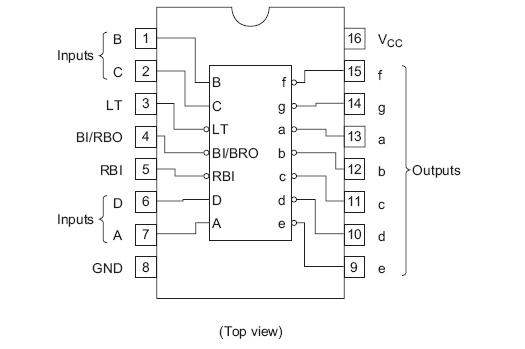
Segment identification and resultant displays are shown below. Display patterns for BCD input conditions. This circuit incorporates automatic leading and / or trailing-edge zero-blanking control (RBI and RBO). Lamp test (LT) of this type may be performed at any time when the BI / RBO node is at a high level. This type contains an overriding blanking input (BI) which can be used to control the lamp intensity be pulsing or to inhibit the outputs.
Ordering Information
|
Part Name |
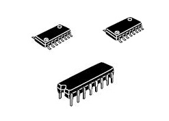
Package Type |
Package Code (Previous Code) |
Package Abbreviation |
Taping Abbreviation (Quantity) |
|
HD74LS247P |
DILP-16 pin |
PRDP0016AE-B (DP-16FV) |
P |
— |
|
HD74LS247FPEL |
SOP-16 pin (JEITA) |
PRSP0016DH-B (FP-16DAV) |
FP |
EL (2,000 pcs/reel) |
|
HD74LS247RPEL |
SOP-16 pin (JEDEC) |
PRSP0016DG-A (FP-16DNV) |
RP |
EL (2,500 pcs/reel) |
Pin Arrangement

Absolute Maximum Ratings
|
Item |
Symbol |
Ratings |
Unit |
|
Supply voltage |
VCC |
7 |
V |
|
Input voltage |
VIN |
7 |
V |
|
Output current (tw £ 1ms, duty cycle £ 10%) |
IO (peak) |
200 |
mA |
|
Output current (off-state) |
IO (off) |
1 |
mA |
|
Operating temperature |
Topr |
–20 to +75 |
°C |
|
Power dissipation |
PT |
400 |
mW |
|
Storage temperature |
Tstg |
–65 to +150 |
°C |


 浙公網安備 33010502000757號